Shrink that prototype
This is a follow on to my last post which was about building a prototyped lithium charging ESP8266 (ESP12) breakout board along with some power management firmware features. Having had reasonable success with the stripboard prototype, the next step was to create a PCB version of this project. PCBs are everywhere and although over time I’ve fiddled around with attempting to fix TVs and stereo systems with varying levels of success, I’ve never designed and created a PCB of my own so this was a completely new discipline to me.
I set myself the goal of trying to make this board as small as possible for no other reason than small is beautiful. I knew that it’s possible to hand make a PCB but I also knew the end result would end up a lot larger (and a lot less pretty) than a machine fabricated board and repeatability would also be a problem. So with the idea of a hand made board dispensed, I set about finding a PCB shop and choosing PCB CAD software.
Choosing PCB CAD software
Also known as EDA (Electronic Design Automation) and ECAD (Electronic Computer Aided Design) software. Everyone likes free but Eagle CAD isn’t really free however there’s a freeware license where restrictions include it being limited to designing small(ish) 2 layer boards for non-commercial purposes. The other package that caught my eye was KiCad which is completely open source and unrestricted. There’s a decent comparison matrix of EDA software here. I settled on Eagle for this project but I’m sure I’ll give KiCad a try in future. Things I did find nice about Eagle were:
- A large user community which means lots of support for part libraries and scripts
- Lots of tutorials available
- It was reasonably easy to get started with for me with no prior Eagle experience and limited electronics knowledge
From what I read the general workflow seems to be similar in most PCB CAD packages:
- Design a schematic by including supply voltage(s), components and wires etc.
- Layout and route a PCB from the schematic created in step 1

I found this sparkfun tutorial very useful as a starting point for Eagle: https://learn.sparkfun.com/tutorials/using-eagle-schematic
Choosing a PCB shop
I started reading this PCB shop comparison guide here and also read a bunch of “arduino create a PCB” and “esp8266 create a PCB” type threads to get a feel for what other people were doing in this area. Following that I’d reduced down to two:
- OSH Park:
- Great automated website
- Lots of online help on the website that really does help eliminate common problems early
- Very open pricing structure
- Free international delivery
- Quick turnaround from order to delivery
- Gold Phoenix:
- Good prices for larger orders
- Lots of flexible options available
- Very quick turnaround
I put together a quick and dirty board design in Eagle approximating the target size of my PCB and sent it to both for a side by side comparison.
With OSH Park I was able to directly upload the Eagle .brd file and get immediate feedback after a minute once their system had performed some basic sanity checks on my design.
With Gold Phoenix I had to work out how to generate gerber files from Eagle, zip these up and submit these to the Gold Phoenix website - a process which is a little bit clunkier than OSH Park but I did get feedback the next day once a human had reviewed what I’d sent.
I’d heard great things about the quality of boards from OSH Park on twitter and also on http://www.esp8266.com/ and the pricing between these two were so close for a small order, I settled on OSH Park - job done.
Schematic recap
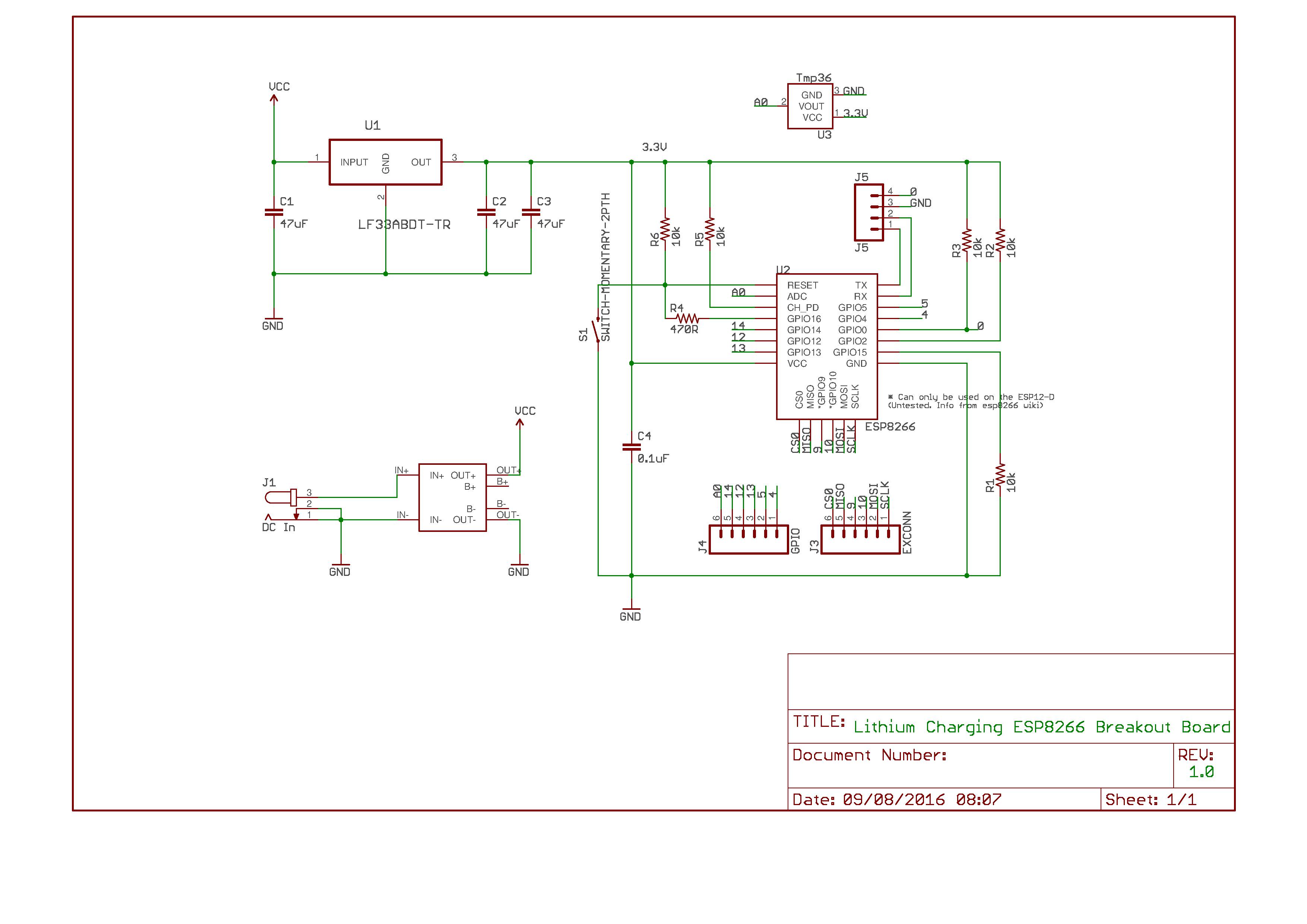
PCB smd parts (mostly)
- 1 x ESP8266 ESP12 board http://www.aliexpress.com/item/Esp8266-WiFi-series-of-model-ESP-12-ESP-12F-esp12F-esp12-authenticity-guaranteed/32468324806.html
- 1 x TP4056 lithium battery charging circuit board(s) with overcharge and overcurrent protection e.g. http://www.aliexpress.com/item/Free-Shipping-5V-1A-Micro-USB-18650-Lithium-Battery-Charging-Board-Charger-Module-Protection-Dual/32453058256.html
- 1 x DC power jack with slotted poles http://www.ebay.co.uk/itm/DC005-PCB-Mount-3-Pins-2-1mmx5-5mm-DC-Female-Socket-Power-Jack-10-Pcs-S9-/231933446157
- 1 x LF33AB smd voltage regulator https://www.aliexpress.com/item/Free-Shipping-3PCS-lot-LF33CDT-TR-IC-REG-LDO-3-3V-5A-DPAK-LF33-33C/32695242320.html
- 1 x TMP36 temperature sensor (optional) https://www.aliexpress.com/item/FREE-SHIPPING-5PCS-TMP36-TMP36GT9-TMP36GT9Z-ADI-TO92/32568770672.html
- 1 x tactile switch https://www.aliexpress.com/item/Promotion-100-Pcs-6-x-6mm-x-4-3mm-Panel-PCB-Momentary-Tactile-Button-Switch/32623137706.html
- 1 x ceramic 0.1uF capacitor https://www.aliexpress.com/item/Free-shipping-1000PCS-100nF-0-1uF-0-1-uF-104-50V-Mono-Monolithic-Capacitors/854151025.html
- Male header pins https://www.aliexpress.com/item/CNIM-Hot-50-Pcs-Single-Row-40Pin-2-54mm-Male-Pin-Header-Connector/32697457200.html
- 5 x 10k smd 0805 footprint resistors https://www.aliexpress.com/item/100pcs-lot-SMD-Chip-Resistor-1-0805-10K-1-8W-100-YAGEO-New-Original-Chip-Fixed/32569368590.html
- 1 x 470R smd 0805 footprint resistor https://www.aliexpress.com/item/100pcs-lot-SMD-Chip-Resistor-1-0805-470R-470-OHMS-1-8W-100-YAGEO-New-Original/32570147477.html
- 3 x 47uF 16V smd 1206 footprint capacitors https://www.aliexpress.com/item/Free-shipping-1206-SMD-capacitor-47uf-16V-476Z-100PCS/32374771833.html
- 1 x Solar panel http://www.ebay.co.uk/itm/161347478808
- 1 x 18650 lithium cell and cell holder http://www.ebay.co.uk/itm/121697118848
- much more patience than last time for soldering these microscopic smd parts
- good quality solder + flux
- tweezers
- ideally something a bit better than the £10 soldering iron I’m putting up with at the moment
- Some people use blue tac for holding the board in place when soldering but I use one of these: http://www.ebay.co.uk/itm/182071028782
A wrong turn
Having previously prototyped the design of this lithium charging esp8266 breakout board on stripboard, putting the schematic together in Eagle was pretty much straight forward - the trickiest part was choosing components matching the specs of what I needed each with the desired and correct footprint size / package for the PCB.
Once the schematic was built, all that was left to do was to layout the components on the board in a semi-neat way and route all traces. Not having done this before I spent a fair amount of time on this stage taking care of the important things including performing many design rules checks (DRC) and electrical rules checks (ERC) along the way in an attempt to head off any problems early. OSH Park provide an Eagle DRC check script and it’s recommended this is used at board design time if using OSH Park and Eagle.
Top tip: print your PCB on paper at 1:1 size to check if real physical components exactly overlay the footprint of the pads / holes on the PCB
A word of warning: the sparkfun page here describes how to setup the Eagle UI to make things easier to use. They also include an Eagle setup script in that page called “spk.scr” which can be used to configure the Eagle UI. This is a useful script however there’s a problem with it: this script switches off layers 25,26,27,28 by default and some library components do drop text onto the tNames layer which will get hidden by this script because that layer gets switched off. This means that if you’re not careful and super alert, there’s a danger you can end up with a PCB silkscreen disaster when the board is later printed at the fab shop because you weren’t aware of all silkscreen text that will be printed.
In the end I edited this spk.scr file on local to avoid this problem reported the issue to sparkfun tech support but as it stands, this problem is still present on their website.
After about a day of playing around all looked good, I was happy with my creation, OSH Park validated the board design seemingly with no issues and I placed an order for 3 boards:

At this point I was excited to have got as far as getting my PCB order in progress and so triumphantly posted to twitter: https://twitter.com/iD8266_1/status/761649736214515713.
Surprisingly that tweet gathered a fair amount of interest including comments from a bunch of good guys highlighting some mistakes I’d made and missed when I was laying out the board:
- The ESP8266 antenna was positioned over copper / traces / the ground plane which would result in reduced WiFi signal strength
- A possible problem with plated slots on the DC jack
- Concerns about use of 0805 footprint smd components being too small to solder by hand
Well that was a bit dire :) My initial excitement wore off quickly and I realised I’d done things in the wrong order..really should have posted the tweet before placing the order. Never mind you live and learn and as it turned out shortly after, I realised I’d made another silly mistake by positioning the TP4056 board rotation the wrong way around. The v1.0 attempt was a disaster of my own creation before it had been delivered and it would be fit for nothing other than soldering practice when it arrived. Undeterred I battled on. v2.0 would be flawless..
Getting it right
The next day I continued on with re-laying out a v2.0 version of the board in hopefully the right way keeping in mind the things I’d learnt from the first early fail. I spent about another half a day switching things around including moving resistors and caps to the underside of the board and of course moving the ESP8266 antenna off the board completely. I decided to stick with the small 0805 footprint components for the moment and also stick with the plated slots on the DC jack and wait for the v1.0 board to arrive before making any further changes. It made sense to wait and see what the v1.0 board looked like in real life to see what else I could learn from that before placing the order for the v2.0 version.
A week or so later the v1.0 board arrived and I saw that OSH Park had done a great job with the DC jack plated slots - hurray a minor win! In fact they’d done a great job overall. The board was very pretty, well manufactured and of very high quality. Shame it wouldn’t actually work. Looking at physical v1.0 also made me reasonably happy with the size of the 0805 component footprints; admittedly they’re very small but doable by hand with a magnifying glass.
A very nice surprise
Along the way, it turns out that OSH Park had been following the tweets going back and forth. Drew Fustini (@pdp7) from OSH Park got in touch, he said he’d been enjoying the tweets about the design of this board and he very generously gave me a $30 voucher to use for my next order and also offered a possible free upgrade to OSH Park swift service if it was available when I placed my next order (worth another $89). Fantastic! This totally took the sting out of the v1.0 fail.
I stared at my v2.0 board layout in Eagle for another hour or so racking my brains for anything that might be not quite right. I tweaked the silk screen here and there and then pulled the trigger on the second order this time paid for with the $30 voucher. Fingers crossed again:

The final build
The 2nd order did get upgraded to OSH Park swift service free of charge and the v2.0 board arrived in record time - 7 working days from when the order was placed. The board looked good and I had all components ready to go so it was time to solder.
I took my time and probably spent about 4-5 hours soldering all of the components onto the board one Saturday afternoon starting with the smallest components first working up to the largest. The small 0805 resistors were tricky to solder and to be honest I’m not proud of how they actually look close up but amazingly I didn’t fry it all into a useless heap of junk and at the end of the day the board did actually work:

What next? The plan now is to continue testing this board (v2.1 needed? not sure) and to find some sort of enclosure for this thing to live in, perhaps an IP rated box for external use.
I also want to test some external I2C devices connected to the ESP8266 to see how this board holds up to hungrier power requirements so some firmware extensions will be needed too.

Comments